- Shanghai Zhongshen International Trade Co., Ltd. - Two decades of trade agency expertise.
- Service Hotline: 139 1787 2118
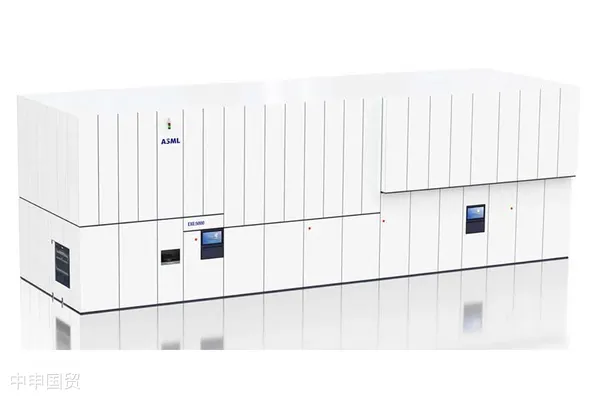
October 10, 2024 News — Two high - numerical - aperture (High NA) extreme ultraviolet (EUV) lithography machines have been successfully installed recently in the factory of a leading chip manufacturer. Each of these two devices is sold at about $350 million and is one of the most advanced and expensive lithography machines in the world at present.

Rapid Deployment of High - Numerical - Aperture EUV Lithography Machines
It is reported that these two high - numerical - aperture EUV lithography machines arrived at the production factory in Oregon, USA at the end of last year and are expected to start production by the end of 2025. These lithography machines are considered an “upgraded version” of the existing EUV technology rather than a completely new product, which makes their launch and adoption relatively fast.
“The high - numerical - aperture EUV lithography machine is more like an upgraded version of the existing EUV lithography machine. We expect it to be launched and applied quickly,” said the companys new CEO in a recent public speech.
Innovative Assembly Method Saves Time and Cost
At the recently held International Optics Conference, the companys new CEO introduced in detail the new assembly method of high - numerical - aperture EUV lithography machines. These devices can now be assembled on - site at the customers location instead of being pre - assembled at the manufacturers site, then disassembled and transported. This method has been successful in dealing with relatively simple deposition and etching tools, and is still being optimized for high - complexity lithography equipment. This move is expected to significantly save time and cost and accelerate the development of high - numerical - aperture EUV lithography machines.
Modular Design Improves Versatility and Efficiency
The main difference between conventional EUV lithography equipment and high - numerical - aperture EUV lithography equipment lies in the lens stack. Through modular design, users can replace different types of lens stacks in the same basic tool, including conventional EUV lenses, high - numerical - aperture lenses and ultra - high - numerical - aperture lenses. This design not only improves the versatility of the equipment, but also brings more cost savings and shorter installation time, thus increasing overall profits.
Stable Power Supply and Efficient Production
The infrastructure required for high - numerical - aperture EUV lithography machines is all in place and running, including a stable 740 - watt power supply, and the power supply capacity will reach 1000 watts in the future. In addition, the photomask inspection system has also been launched to ensure that the equipment can be put into production without excessive auxiliary support.
High Mask Size Breaks Through Chip Performance
Last year, a chip process expert proposed the idea of expanding the mask size from 6 inches × 6 inches to 6 inches × 12 inches at an international conference. This year, this technology has received strong support from several photomask infrastructure companies. The company stated that adopting a double - sized mask is an easy breakthrough for the industry. It is expected to overcome the limitations of high - numerical - aperture technology in chip size and achieve a 40% performance improvement.
High - Numerical - Aperture Lithography Machine Accelerates Production
Another lithography director revealed that two high - numerical - aperture EUV lithography machines have been installed in the production plant in Poland. These two systems demonstrate significant improvements compared to standard EUV lithography machines, and the installation speed is expected to be faster than that of the first one. All necessary infrastructure is in place, and the photomask inspection system has also started to operate, enabling the high - numerical - aperture EUV lithography machine to be put into production more quickly.
Industry Response and Future Outlook
Although some chip manufacturers have postponed accepting high - numerical - aperture EUV lithography machines on the grounds of cost, industry analysts predict that with the continuous progress of technology and the improvement of production efficiency, these manufacturers will have to follow suit to maintain their competitiveness in the industry. In addition, there are rumors that the introduction of high - numerical - aperture lithography machines will help overcome the current technical bottlenecks and promote the continuous development of Moores Law.
The introduction of high - numerical - aperture EUV lithography machines and the overall technological progress at this conference are regarded as good news. It not only helps to improve the accuracy and efficiency of chip manufacturing but also has a positive impact on the stock prices of related equipment manufacturers. With the increasing demand for advanced lithography technology in the global semiconductor market, the successful deployment of high - numerical - aperture EUV lithography machines will further consolidate its leading position in the industry.
Related Recommendations
Contact Form
? 2025. All Rights Reserved. 滬ICP備2023007705號-2  PSB Record: Shanghai No.31011502009912


